Basic building blocks for integrated circuits (IC), very large scale integrated circuit (VLSI)
And ultra large scale integrated circuits (ULSI) are diodes and transistors. Large numbers of this diodes and transistors are fabricated together in a tiny piece of silicon wafer to make the IC/VLSIC/ULSICs.
Semiconductor Integrated Circuit (IC) Manufacturing Process
Let’s assume we have to fabricate a chip which consists of a single N-P-N transistor, the steps typically are:
1. Sand to impure silicon: Sand or Silicon dioxide or Silica (SiO2) is mixed with carbon and heated above 2000 degree C. to get metallurgical grade silicon (97% purity).
SiO2 + 2C = Si + 2CO
2. Impure silicon to pure polycrystalline silicone: The semi-pure (97%) silicon is then powdered and first reacted at 300 degree C with gaseous hydrogen chloride (HCl) to make tricholorosilane (SiHCl3).
The tricholorosilane is then vaporized and reacted with hydrogen gas at 1100 degree C to get 99.999% pure polycrystalline Silicon (or Polysilicon).
Si + 3 HCl = SiHCl3 + H2
2SiHCl3+ 2H2 = 2Si + 6 HCl
Although its 99.999% pure but polycrystalline silicon is useless for chip fabrication, it needs pure crystalline silicon.
3. Polycrystalline to pure crystalline silicon ingot: Czochralski process is used for making pure N-type or P-Type silicon crystal ingot from polycrystalline silicone. The process is diagrammatically shown below:
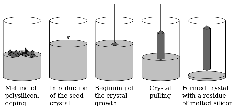
Image source: Wiki
We have to make P-Type crystalline silicon ingot through this process for the purpose of making our N-P-N transistor chip.
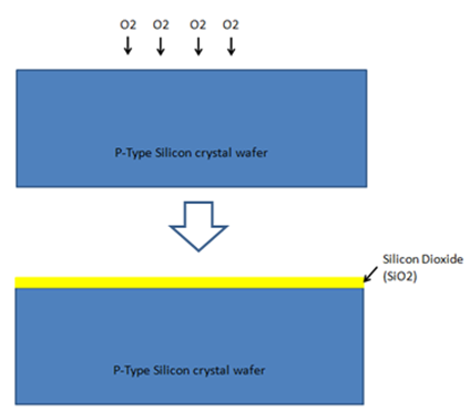
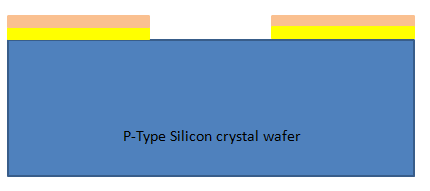
4. Ingot to wafer: The P-Type silicon crystal ingot is sawed into thin silicon wafer.
5. Oxidization: The clean wafer is exposed to oxygen to convert the top layer into Silicon Dioxide film.
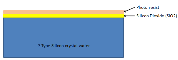
6. Applying photoresist layer: Thin photoresist material layer is then applied:
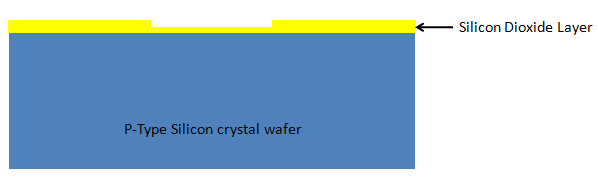
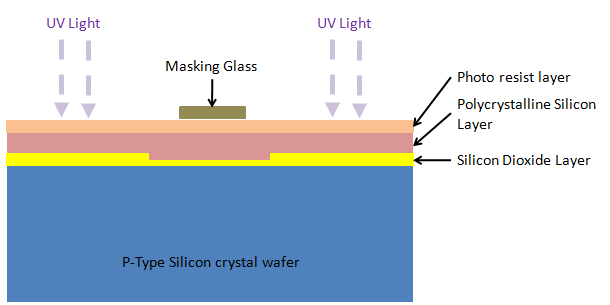
7. Glass masking: Glass masks are used to selectively expose the desired portion to the UV rays, the process is called photolithography:
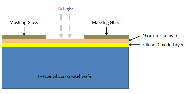
The UV rays soften the exposed photoresist areas, rest of the areas remain hard.
8. Etching: Special chemical is used in this process to remove the soften exposed photoresist portion:
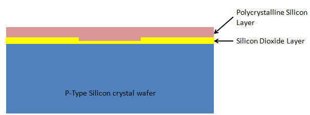
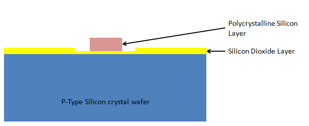
9. Applying Silicon Dioxide Layer: Another thin layer of silicon dioxide is applied over the exposed portion of the wafer:
10. Polycrystalline silicon layer: Polycrystalline silicon layer is applied over the SiO2 layer:
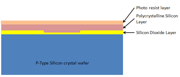
11. Applying another photoresist layer: One more photoresist layer to be applied over the polycrystalline layer:
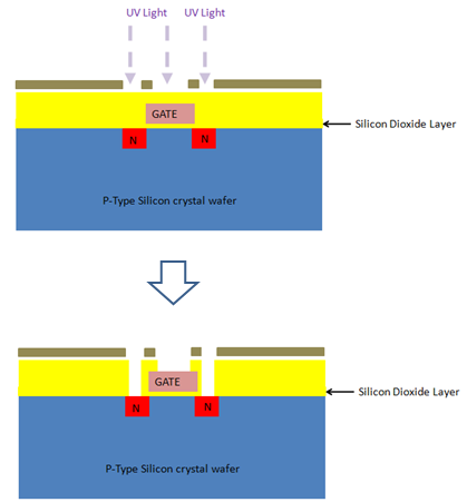
12. Photo lithography – Second time: Glass mask and UV lights are used for the photolithography for the second time:
13. Etching – Second time: Etching process is carried out once again:
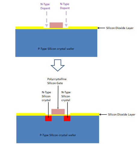
14. N-Type Dopant implant: N-type Dopant materials (e.g., Phosphorus/ Arsenic) gas is used for implanting the Dopant to the suitable zones:
15. Applying silicon dioxide layer – Third time: Another layer of silicon dioxide or glass is applied all over:
16. Photolithography – Third time: For etching the required areas, again the photolithography is to be carried out, which will produce output like:
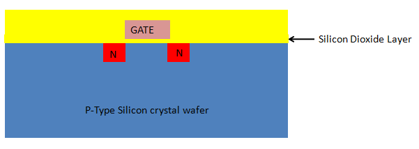
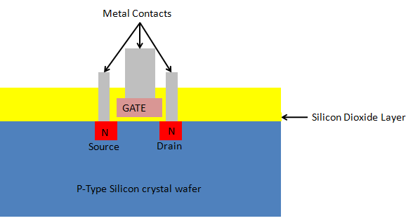
17. Making contacts : Metal layers are deposited to make the necessary contacts with the source, drain and gate of the final N-P-N chip:
Through this integrated circuit (IC) chip fabrication process we would be able to manufacture a chipset which consists of single N-P-N transistor. Actually the basic processes or steps for fabricating complex VLSIC or ULSIC chip is similar only repetition and scale changes.