What is semiconductor?
Semiconductor is the basic building block for modern day electronics.
As the name suggest, the conductivity of semiconductor is in between that of metallic conductor and non-metallic insulator.
Any electronic components made up using semiconductor is called semiconductor devices. Diodes, transistors are basic semiconductor devices. Integrated Circuits (ICs), Very large scale integrated circuit (VLSI) and Ultra large scale integrated circuit (ULSI) are complex semiconductor devices.
Physics of Semiconductor Devices
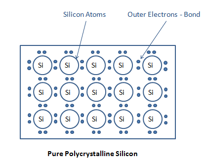
Semiconductor is made by using non-metallic silicon (Si) as base material and then by injecting doping material (or dopant) into it.
The dopants could either be Phosphorus/Arsenic or Boron/Gallium.
Phosphorus /Arsenic have 5 electrons in its outer orbit.
Boron /Gallium have 3 electrons in its outer orbit.
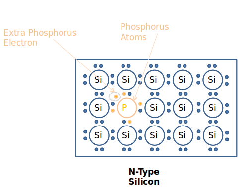
N-Type Semiconductor
The silicon which is dopped by Phosphorus (P)/Arsenic (As) (5 outer electrons), are called N-Type semiconductor, get one free electrons for each doping material atoms as all the silicon atom has 4 electrons in its outer orbit and the Phosphorus/Arsenic atom have 5 outer electrons. The extra electron carries electricity for N-Type material.
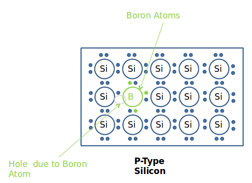
P-type Semiconductor
In case of P-type, dopant is Boron (B) (3 outer electrons) and electricity is conducted by deficit of electrons or Holes.
Diode
Diode is the simplest semiconductor based device, where half of a N-Type Silicon base is doped with boron (B). Thus the N-Type and P-Type semiconductor stays side-by-side to make a PN diode.
The peculiar characteristic of a diode is that it allows current to flow in one direction and blocks in other direction.
For the current to flow, the P side of the diode has to be connected with the +ve terminal of the battery and N side with the –ve.
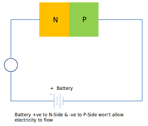
Otherwise current won’t flow.
From the above figures, you can see that a diode allows the current to flow only in one direction, this is reason it is used to protect electronic circuit from opposite current flow.
Transistor
The semiconductor device where the N-Type and P-Type semiconductors are connected in either N-P-N or P-N-P fashion, it is called transistor.
The middle piece of semiconductor is called base, the other two is called emitter and collector.
Speciality of transistor is that the current always flows through transistor only after allowing little current to the base.
For the transistor to work – base to emitter to be forward biased (P side to be connected with the battery +ve and N side to be connected with battery –ve) and base to collector to be reverse biased (opposite to forward bias). Confused?
See the correct connection (biasing) for PNP and NPN transistor as shown below:
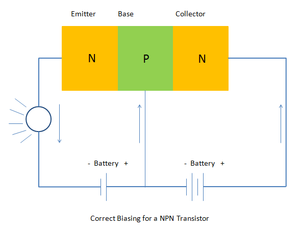
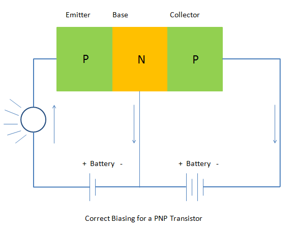
As you have seen, that for the transistor to work i.e, flowing of current between emitter and collector you need to apply little current between base and emitter, hence transistor can be used as switch. Another application of it is as amplifier.
Hi, I am Shibashis, a blogger by passion and an engineer by profession. I have written most of the articles for mechGuru.com. For more than a decades i am closely associated with the engineering design/manufacturing simulation technologies. I am a self taught code hobbyist, presently in love with Python (Open CV / ML / Data Science /AWS -3000+ lines, 400+ hrs. )